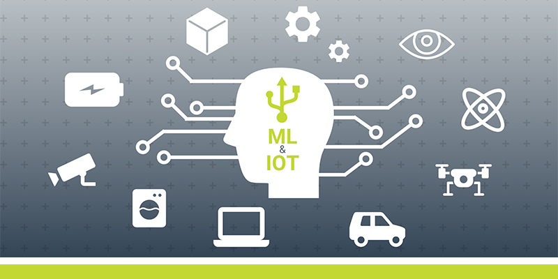
Many of you may be familiar with the concept of “intelligence at the edge” in IoT. Usually, such a reference is connected to having some sort of edge-based processing capability in a gateway. However, the world of Machine Learning (ML), formerly the domain of large computing facilities, is moving heavily into the world of IoT.
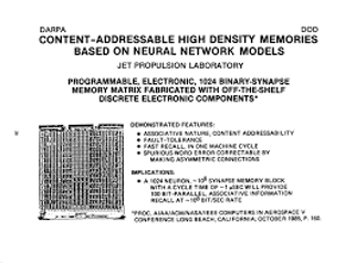
I remember back in the mid-1980s being a young electrical engineer at the Jet Propulsion Laboratory in Pasadena, CA. My first exposure to ML was when I was asked to produce the hardware for something called a “neural network” for a team led by Prof. John Hopfield at CalTech so researchers could use it for scientific investigation. The resulting end-table sized wire-wrap board represented only a 32 “neuron” neural network with a 1024 programmable binary connection network. An old photo of that hardware is below:
Things have come a long way since that time. By way of a bit of housekeeping, in the following, I will be using the term “constrained” in the context defined by the IETF in RFC7228bis back in 2014.
Using ML today can be divided roughly into two sections: training and inference. Training involves the use of statistical algorithms to learn from existing data resulting in a model. Inference is the use of that model to make decisions on new data. In the last few years advances in low power processing capability, coupled with improvements in wireless radios and battery technology, have gone a long way to provide the hardware basis for ML inference to be executed in battery-operated sensors and other highly constrained devices (ok, perhaps not constrained compared to the dinosaur hardware above, but certainly compared to normal cloud-based computing resources). A great example can be found in the O’Reilly book TinyML by Pete Warden and Daniel Situnayake. In that book, they describe how Google engineers in 2014 were running neural networks only 14kB in size on Android phones. Those engineers had to use the small DSP unit in the phone to continuously listen for “OK Google” as the main phone CPU needed to sleep to conserve power. That is an amazingly small amount of memory needed to provide such a powerful feature doing something as complex as recognizing a spoken phrase.
New approaches to old problems have made great strides in pushing cloud-based ML inference into those selfsame highly constrained devices.
TinyML
One of the approaches that is working to fundamentally change sensor-based systems is referred to as TinyML. With a generally defined goal of running a neural network model with an energy cost under 1 mW, TinyML techniques enable a whole new class of capability and operation in low power wireless sensors and other constrained devices. At this point, I cannot remember exactly how much power that old neural network board I made consumed, but it was thousands of times more than the TinyML goal.
Using the TensorFlow Lite for Microcontrollers framework, software developed using that framework can run on embedded devices with only 10’s of kilobytes of memory with inexpensive platforms, such as the SparkFun Edge, Arduino Nano and the STM32F746G Discovery Kit readily available to experiment with.
Getting started with a TinyML project is simple. Order one of the above boards and go to TensorFlow.org for Mobile and IoT (https://www.tensorflow.org/lite/models) as you wait for it to arrive. There you will find pretty much everything you need to develop models and run them on your test platform using the TensorFlow Lite for Microcontrollers toolset. You will also find a number of ready-to-use solutions for tasks such as image classification, object detection, etc. TensorFlow Lite for Microcontrollers is written in C++ and can be included in any C++ 11 project to be run on a 32-bit platform. The first time you recognize or classify an image or perform some other ML task with one of these setups you will be hooked!
However, if the thought of striking out on your own feels daunting, companies like Edge Impulse (https://edgeimpulse.com/ ) make it even easier to utilize TinyML in your next project.
AtomBeam
Another way to utilize advanced ML techniques in a constrained environment can be found in AtomBeam’s (https://atombeamtech.com/ ) approach. AtomBeam technology is focused on enabling the lossless compaction of data sent through a communication channel with effectively zero latency in constrained environments where compression techniques are not viable or beneficial. By learning data from an operating communication channel and using it to train a model in the cloud, the resulting model can then be placed into an IoT sensor to achieve enormous bandwidth savings (reducing data sent over the air by 75% or more while still transferring all of the data). This enables either more data to be sent over the same channel, more devices to be supported, or simply saves 25% or more of the battery power used to transmit the uncompacted data. Their current executable image is only 1.3 kB and requires no special hardware resources, which makes it highly suited for constrained environments. They have even made the learning phase simple. Just upload your captured communication channel data to their cloud-based application and it returns a model for you to use with their library code. They have also recently gone further and created a generic compactor that requires no learning phase, and still provides a 50-60% compaction of data in 2 kB of code/data memory.
Of course, combining a TinyML use case with the AtomBeam use case would result in a highly capable but still low power IoT sensor. As other ML-based approaches are brought to market, these combinations of capabilities will make the next generation of IoT sensors many times more capable than they are today. I predict that in the future, creating a smart endpoint will revolve less around CPU selection and creative power management approaches and more around determining the precise mix of ML-based capabilities needed for the device to fulfill its intended purpose.
About The Author

David Smith
VP of IoT Solutions
Dave Smith is the Vice President of IoT solutions with responsibility for technical advisement and thought leadership around products, solutions, and services; both inside and outside of the GetWireless portfolio. Dave is a tenured information technology professional skilled in LPWAN, IoT, Wireless Technologies, Telecommunications, Software Development, Testing, and Embedded Systems. David began his career at NASA’s Jet Propulsion Laboratory and prior to joining GetWireless served as CTO and Director for two Innovative IT and IoT hardware manufacturer’s in the Twin Cities area.